
I need a minimal-lag zero-cross detector for the tone control section of an audio preamp which will rely on digital potentiometers for adjustment. The pot adjustments (communicated from an MCU over SPI) need to be sync’d to 0V input to avoid popcorn noise.
The digital pot has a write-inhibit input that can be driven low to latch the adjustment while the input signal is crossing 0V. My goal is to hit this pretty close to the mark (±100mV), for any audio-rate signal, which may be up to 3.5 Vrms (~10 Vpp) and 20 kHz. To be valid, the signal needs to remain low for 25ns. I’d like to hit this with room to spare and also minimize signal bounce / glitching for a slowly-changing audio-rate input.
A new comparator IC by Texas Instruments that makes this possible with high resolution and minimal phase lag is the TLV1871. The whole TLV18xx family of comparators is fairly new, and this is one of the newest, and I think the most exciting. (I think it has only really been on the market in “Active” availability and in-stock at Digikey or Mouser for the past year or so, after being in Preview for a while.)
Target design requirements
The zero-crossing detector design must:
- Support 10 Vpp (3.5 Vrms) input signals; register “near zero” across the audio rate frequencies, 20 Hz — 20kHz,
- produce a 3.3V, active-low output, and
- include a “force low” digital control input to override this circuit.
- The active low pulse should be at least 1µs wide, and
- register a zero-crossing window when the signal is at 0V ± 100mV.
- Finally, the circuit and its ICs must operate on a ±12V analog domain power supply. A separate +3.3V power supply for the output signal and digital logic is also available.
Related work
Rod Elliott, author of the incomparable ESP Audio pages, has an application note about zero-crossing detectors that is worth reading first (giving several options for ZC implementations for both small-signal as well as A/C power measurement), as well as a page on comparators with a zero-crossing circuit example.
The comparator-based circuit shown in the ESP app note uses the LM393, and has approx 1.3 µs (per datasheet) propagation delay at 100mV input overdrive. Rod writes, “It’s capable of achieving a pulse width of around 70µs, faster than any other I’ve seen.” Rod also cautions that keeping the Vcc – Vee delta tight is important to enable a quick output transition time, even with a fast output slew rate. As we will see, the TLV1871 can offer much faster performance.
The TLV1871 comparator
The TLV1871 is notably a push-pull comparator (no pull-up resistor needed), with wide Vin (up to 40V), and split input and output rails — so you can use (for example) ±12V for Vcc/Vee on the input side and +3.3V / GND on the output side. There is no need to divide down the input signal with resistors unless it’s really, really high voltage. Propagation delay is dependent on input overdrive but TI quotes 100ns at 10mV and just 65ns at 100mV. The LM311 also has split input/output power supplies (more on this device later) but the TLV1871 is the only push-pull CMOS device I’ve seen with split input/output supplies and 36V+ tolerance.
Circuit schematic
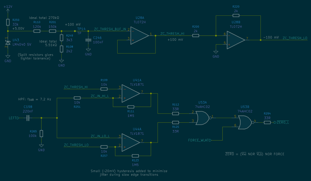
This circuit meets the requirements described above, with two TLV1871’s and 1/2 SN74AHC02 (quad NOR-2 IC) per channel. Only a single NOR gate would be needed if I didn’t also need to include the “force ZC signal.” One channel is shown. If you need two channels for stereo processing, they can share the same threshold buffers. Positive feedback provides about 20mV of hysteresis to avoid slow-signal output glitches.
This has an active low output but the “true zero cross” intermediate output (computed by U53A) is active high. Alternative forms of this circuit could involve swapping the sense of the two comparators, and switching the combinational logic from NOR to NAND, etc. as you might require.
This uses a ±100mV band for the “near zero” region, which could be made arbitrarily smaller for tighter output pulses. The highest-frequency zero-cross you want to detect dictates how wide that needs to be. The limits as-established are designed to produce a 1.4 µs pulse for a 20 kHz, 2 Vpp sine wave input (verified by SPICE simulation).
The +100mV threshold is established by using an LM4040 5V Zener diode and a resistor divider. The bandwidth can be adjusted by tuning the resistors. This high-impedance signal is buffered with 1/2 of a TL072H dual op amp, and the other half is used in inverting configuration to produce the -100mV band. The LM4040 was selected less for its precision and more for its ability to operate at low current (only 100 µA is required over the cathode to establish the 5V level); most regular Zener diodes require an IZT of 5 mA. A less-expensive voltage reference could be used at the expense of higher power draw and lower absolute DC accuracy.
There is a dual (TLV1872) package that could conceivably merge the two comparator sections into one IC, but the minor downside of these IC’s (for the amateur, anyway) is that TLV1871 comes in the SOT-23-THIN-8 package (which is not too bad to assemble, especially with hot air), but TLV1872 only comes in VSSOP-10 (no thank you).
The power supply connections for the TLV1871 use separate input and output supplies, like so:
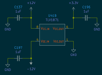
The TL072 has the usual ±12V rails and decoupling capacitors; not shown.
Simulation and testing
This circuit was simulated in ngspice using TI’s SPICE model for TLV1871. A range of input signals from 1 kHz to 20 kHz were tested at 1, 2, and 10 Vpp using transient response simulation. Results are as follows:
- The TLV1871 model appears to show about 100 to 180ns propagation delay.
- The minimum input overdrive requirement is ~5mV (slightly more than Vos)
- At 2Vpp sine, 1kHz, we see the output signal low for ~30 µsec.
- At 2Vpp sine, 20kHz, we see the signal low for ~1.4 µsec.
- At 10Vpp sine, 20kHz, we see the signal low for ~260 ns.
- We need a minimum of 25ns hold time for ~WLAT to trigger on the digipot. This simulation shows we will meet that timing, even with large error bars on true signal propagation delay.
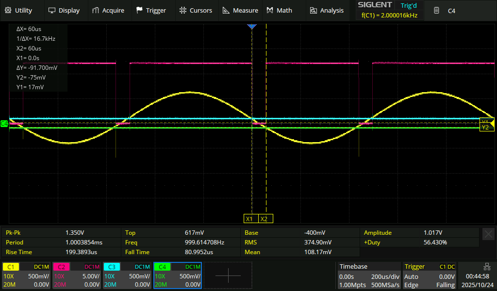
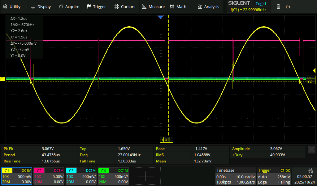
A circuit assembly was also tested on a breadboard. Power was supplied from a benchtop power supply and measurements were taken with my Siglent SDS2104X Plus oscilloscope. As the propagation delay on this circuit is incredibly fast, this will give you as tight a zero-cross pulse as you could want. The circuit produces a decisive logic-low signal when the input AC waveform crosses 0V. Here it’s showing ~60usec pulses for the ±100mV zero-cross interval with a 1 kHz input of 1 Vpp; a 6% duty cycle:
On the bench, this reliably produces clear output signals when the input is up to 17 kHz. Beyond this point, capacitive coupling, crosstalk, noise, and all the other fouls of breadboard work makes the circuit unreliable, and spurious output glitches appear at times even when the input signal is nowhere near the zero-cross window. A PCB will be needed to test the remainder of the target frequency range but given the on-breadboard performance at up to 85% of the target frequency, I am pretty confident it will function across the full 20kHz range, given a proper ground plane and lack of flying wiring. What can be discerned on the oscilloscope at 20 kHz appears to be an output-low assertion of 2.0–2.7 µsec (1–1.5% duty cycle), which is more than enough margin of safety to be able to hit the mark on a PCB.
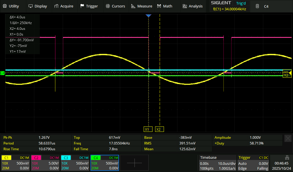
My original design called for only 10mV hysteresis (provided via 3.3 MΩ resistors). The circuit measurements showed a lot of noise and glitching outputs, and doubling the feedback current (resistors adjusted to 1.5 MΩ) helped quiet this down significantly. The 20mV hysteresis does mean that the effective window size is visibly asymmetric at higher frequencies. In Figure 4, the “falling edge” zero window in the center of the screen capture is 4 µsec wide, whereas the rising edge of the audio waveform that follows is only 3 µsec.
Both windows have some visible phase lag relative to when the input signal appears to cross the ±100mV guard band. The falling edge of the audio signal dives below +100mV and the output signal asserts low approximately 800ns later. I believe the propagation delay would be lower on a PCB, as the circuit is up against significant stray capacitance on the test breadboard. While higher-amplitude input signals move through the ±100mV band more quickly than a lower-amplitude signal (and thus have less “valid time” for the signal to assert low), the greater dV/dt means the comparator experiences a stronger input overdrive, which leads to much tighter propagation delay. For example, we actually acquire valid pulses (at just 1.2 µsec pulse width!) for 23 kHz with a 3 Vpp input signal:
Moving back to the 17 kHz signal analysis: The rising edge window has greater phase lag to it, starting the pulse late, due to the 20mV shift from hysteresis in the effective window band limits. This should actually help the falling edge of the output pulse align closer to true 0V, but it is also “valid” (low) for about one microsecond after the audio signal rises above the +100mV guard band. As it’s the falling edge of the pulse that latches the digital pot which is the target of this application, this is not a concern.
If you dial down the window bounds (and maybe use less hysteresis feedback, balanced against good analog layout technique) I believe you could achieve pulse widths under 1 µs if you need it, especially with a high amplitude input. With a 3 Vpp signal, falling-edge zero-crossing events were registered above 60 kHz, but the 20 mV hysteresis shift caused rising edge events to disappear above 23 kHz.
The LM311 comparator
As an alternative to the IC used in the circuit shown above…
If you don’t want to handle a tiny surface mount IC, the LM311 chip is an older comparator with both open collector and open emitter on the output side so you can ground the emitter and pull up the collector to 3.3V, while supporting inputs up to +/-18V. LM311P is a PDIP-8 single; LM311 and its wider-temperature-range counterpart LM211 are also available in SOIC-8 or TSSOP. This is a somewhat faster device than another classic PDIP comparator like the LM393 (datasheet-declared propagation delays are between 100–200ns), but it’s no TLV1871, so its performance would be somewhere between the two. It also consumes 6x the LM393’s quiescent current. (5mA typ, 7.5mA max, w/ no load!) The TLV1871 is a modern CMOS device and over the full temperature range, its Iq,max is just 140 µA. Finally, the LM311 also requires drawing a current through a pull-up resistor when asserting the output, and getting snappy turn-off times means that would need to be a fairly strong pull-up: 3.3V into 1 kΩ would be over 3mA, 470Ω would be 7mA.