
My Eurorack-compatible synth project requires a ±12V power supply. I also wanted to use an external “power brick”-style AC-DC converter to handle the mains power. I developed my own secondary DC-DC power supply with two LDOs, a Ćuk inverting regulator, and a power distribution bus to clean up the output of the power brick and generate the dual-sided power supply required by the rest of the system.
In developing the power supply for my system, I had the following initial requirements:
- Generate ±12V power rails for use by the modules (a common +5V rail is optional).
- I was uncertain of the total power required, so being oversized wouldn’t hurt.
- Handle AC/DC conversion via an external power brick.
- Final power regulation stage should be linear for as internally-quiet as I could get the power rails.
- Introduce as little additional switching noise as possible for voltage inversion.
- Embed the power distribution bus that has plugs for every powered component in the system (at least 12 modules).
The rationale behind using an external power brick was two-fold: First, I didn’t want to work with mains power myself. I could have added a power-entry module to my enclosure and wired that to an internal PSU like a MeanWell RT-65B, but my second requirement (or at least, preference) was that this be physically separated from the main enclosure. My wall power is noisy and I wanted that on the other side of a large ferrite choke from the rest of the system.
(The RT65-B in particular would also violate the linear PSU principle, as it would deliver ±12V directly via switching supplies. That said, in hindsight, it would have been a helluva lot easier and cheaper to just throw one of those in here and move on. But then, pretty much everything about this synth project is both overkill and unnecessarily complicated; rational decision making was never the point. This whole project is going for style points.)
At this stage of the project I wasn’t sure exactly how much power I would ultimately need. In the final analysis, it’s now looking like I need approximately 12W of power delivered to the modules; a supply rated for a total of ~20W would probably be plenty. At the time I started working on this PSU, though, I wasn’t at all confident about that and thought that I should aim for at least double that size, to be safe. The 1/2 A max on the -12V rail of the RT65-B would also likely be adequate for the final result, but I was also uncertain about the ratio of power needed on +12V vs -12V too, as I had several more modules to design in the future, so I wanted to make sure the -12V rail would handle at least 12W directly. My design target was 3A (36 W) on +12V and 1A (12 W) on -12V, for a total of 48 W of delivered power.
Because I wanted to use a linear regulator to deliver the +12V bus, that meant I needed an AC/DC converter that would provide some DC voltage greater than that; enough to supply any necessary dropout voltage for a linear regulator.
I eventually opted for the MeanWell GSM60A15-P1J, which delivers 60 W of power (4 A) at 15 VDC. It’s reasonably compact, affordable (about $23), and had an amount of power that seemed adequate under the most conservative modeling of power demand assumptions I could make. It also used a 2.1mm ID barrel plug, which would make the corresponding jack on the enclosure easy to source. If I ever wanted to use a different power brick, I’d be able to find one of whatever necessary wattage with the same barrel plug.
Now I was faced with the challenge of developing regulator circuits to convert 15 V to +12 and -12 V. The 15-to-12 circuit would be a very straightforward linear regulator design; the most complicated tasks there were picking an appropriately-sized heatsink, and also rigging up a soft start to prevent too-high of inrush current. You can’t just add a linear regulator to get -12V though; I would need some sort of switching stage to go from +15 to a lower voltage (e.g., -15) and then use a negative LDO to smooth that out at -12V.
The final system has five major elements:
- Input protection, for reverse polarity, overvoltage, and overcurrent / short-circuit protection.
- A linear regulator producing +12V from +15V.
- A switching Ćuk converter regulator producing -13.5V from +12V.
- An LDO that drops from -13.5V to -12V.
- Output distribution and bulk decoupling.
Input protection
Upstream power enters the module through a 2-pin Molex MicroFit 3.0 cable and jack, or via a pair of posts (Mill-Max 3233-2-00-15-00-00-08-0) that a benchtop PSU could hook to directly via alligator clips. The input protection subcircuit immediately follows. Given that I would be using this assembly with all manner of other electronic modules in various states of readiness, I tried to engineer as much fault tolerance as possible into the circuit.
- Reverse polarity protection is provided by some SX33 Schottky diodes immediately following the input. Paralleling a few of these enables them to handle plenty of current and also keeps the Vf low (to save headroom for the 12V LDO). In hindsight, rigging something up with a PMOS FET would have had a lower R_on and probably would have been a cheaper and more-compact choice, but it’s difficult to find MOSFETs without body diodes that would enable current to flow in the reverse direction.
- The main protection comes from a TI TPS2421 eFuse IC. The eFuse monitors the current admitted through and shuts off the output if an overcurrent condition is found. Overcurrent is programmed by an external timing capacitor. Given that I had fairly large bulk decoupling on the distribution side, I needed to balance the ability to accommodate that with the desire to shut off quickly if a short circuit developed. I was eventually able to set this at a 5A limit, in part by adding soft-start circuitry to both power rails to limit the inrush.
- The eFuse also offered an external ~EN pin, which I could take advantage of for overvoltage condition-lockout. An LM211 comparator compares the input voltage through a divider to a fixed 6V Zener reference voltage; the divider is such that if the input voltage exceeds about 16V, the comparator drives ~EN high and cuts off the output current of the eFuse.
+12V Linear Regulator
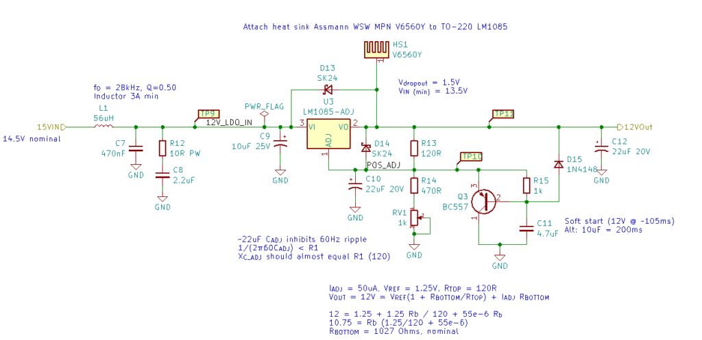
The Schottky diodes for reverse polarity protection and the R_on of the eFuse mean that at max draw, the input to the LDO would be about 14.5V. I chose the TI LM1085 IC for the +12V regulator for a few reasons:
- It has lower dropout voltage (about 1.5V) than some older but widely-chosen options like LM317, which is safely below the range of the post-protection input voltage.
- Supports up to 3A of current
- TO-220 package is easy to solder and easy to attach an appropriate heat sink.
- Still fairly inexpensive
There are “better” LDOs that handle similar or better power loads, with even lower dropout voltage, but they often require much smaller surface mount components. Given that I couldn’t easily find an AC/DC converter of the appropriate wattage in any voltage between 12 and 15V, selecting one of these wouldn’t have offered any real benefit, as I would still need to burn off 2.5–3 volts to get to a 12V output either way.
The LDO design itself is conventional. The only elements worth remarking on are the LC input filter with RC damper design on the upstream supply, and the BJT-driven soft-start circuitry on the output which stretches out the startup over about 100 ms.
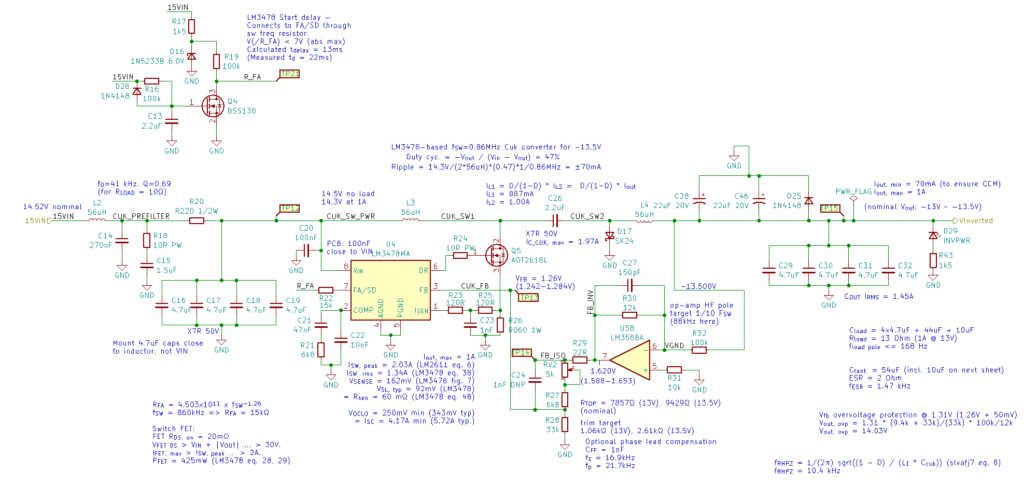
Inverting Ćuk Converter
The most interesting part of the system design is the inverting switching regulator. This uses the Ćuk topology, named after its inventor, former Caltech professor Slobodan Ćuk.
Ćuk converters are interesting because they natively invert the voltage, and as such can go from “low” to “high” voltage (e.g. +5 to -12V), from “high” to “low” (+12V to -5V), or anywhere in the middle. The design is a switched capacitor topology, which also provides excellent isolation of the input and output of the power regulator. While the Boost converter topology can generate a lot of RF noise on its output, and Buck converters can inject a lot of noise back on the input power bus, Ćuk converters are typically less noisy on both sides, due to the filtering effects of the built-in inductors on either side of the flying capacitor.
The main downside of the Ćuk converter is that it is somewhat more obscure than Buck or Boost topologies, so there are fewer resources to learn about it, calculate loop stability criteria, and so on.
The easiest way to integrate a Ćuk converter is the TI LM2611 IC. This is a complete regulator and you can follow the equations in the datasheet to size the two inductors and the flying capacitor to get up and running very quickly.
Unfortunately, the LM2611 has a max input voltage of only 14V! We’re just a bit over this maximum. I could have figured out how to burn off 1V from the input, but it would also be marginal to handle the power requirements of the overall circuit. Even though the “A” grade advertises a 1.2A max, this is actually the switch node current rather than the delivered current. The ultimate power capacity is dependent on both the input and output voltages, as shown in a set of figures buried several pages deep in the datasheet. Figure 22, for Vin = 12V, is most relevant here:
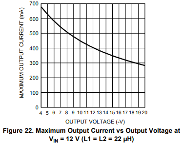
Even under fairly light loading assumptions, the 400mA limit at -12V felt very skimpy. I wanted to guarantee more capacity than this. Moreover, if I wanted to use an LDO to provide -12V, I would need to give that some headroom, using the Ćuk converter to generate around -13.5V, which would further reduce the ampacity of the circuit. So I needed to develop a Ćuk converter circuit with an external switch FET.
Fortunately, while examples of Ćuk converters, or the equations needed to design one, are fairly few and far between, TI’s excellent online library continues to deliver. Reference Design PMP30487 shows how to repurpose the LM5022 Boost controller IC to build a Ćuk instead.
I selected the similar LM3478 Boost Controller for use in this circuit, and an AOT2618 MOSFET for the switch. The TI design has some different requirements: a -36V target, and 50W of capacity, so some of the decisions made in that circuit could be scaled down. It does, however, provide some neat insight into how to make this work.
For high-wattage Buck or Boost conversion, you typically use a Buck or Boost “controller”, which is most of the necessary circuit that you’d find in something like a “Simple Switcher” LM2679. But the actual power being regulated doesn’t flow through the controller; instead, you provide an external power MOSFET (which can handle 10’s of amps), and the controller drives the gate pin to control the switching. As in any other regulator circuit, the controller receives feedback from the output circuit, typically trying to keep its FB pin at a specific low voltage like 1.2V. If the voltage falls below this threshold, it turns the switch on to enable more power to flow through; if the voltage rises higher, it cuts off the output current.
This is well and good, but directly controlling an inverting supply can’t work the same way. If the output voltage is supposed to be -13.5V, I could divide that down to -1.2V, but that’s still on the wrong side of GND for the controller! Analog Devices has a fancy controller part that would automatically work with either +1.2V or -1.2V, but it was both expensive, and (more importantly) required finer-pitch soldering than I wanted to do. Fortunately, the TI system design had an elegant solution: invert the feedback with an opamp.
The fact that this could work made my head spin a little bit. If I was in a regular audio module, sure. But I don’t have a working negative supply rail at this point in the circuit, so how can I invert a negative voltage with an op-amp running on a single-sided supply? Two reasons:
- The input is negative, so the output is positive, and therefore within the supply range of the op-amp.
- The op-amp topology is inverting, so no matter what the voltage is of the regulated supply output that we’re sensing, both op-amp input pins will always be held at virtual ground, which does not violate the input common mode range.
This is one of the few times I used the LM358BA op-amp; in particular because I need to run this circuit single-sided (so Vss is GND) and the input will also be at GND; and unlike the TL072, the LM358 has a common mode input range that works down to its Vss.
There were a few other elements to work through as well. The LM3478 uses a current-monitoring feedback loop as well, which can provide some short-circuit protection, which requires a power resistor below the transistor. A 60mOhm 1W resistor worked fine here for keeping the circuit running without hiccups.
The compensation network connected to the COMP pin of the LM3478 was also a source of mystery regarding the appropriate values. The challenge is to pick a cutoff frequency that is above the load pole, but well below the right-hand plane zero (RHPZ) in the frequency response of the overall Ćuk converter.
The RHPZ frequency can be calculated with 1/(2pi) * sqrt( (1-D) / (L_1 * C_cuk) ). In this circuit’s case, that is 10.4 kHz. (The LM2611 datasheet is a good reference for calculating things like the duty cycle of the Ćuk.) Meanwhile, at the full 1A output, the load pole would be 168 Hz.
The ideal compensation network frequency is greater than 2x 168 Hz, and less than 1/10 of 10.4 kHz — so 500 Hz would be a good value. I used TI Power Designer 5 to generate a Type II compensation network targeting this frequency, consisting of C21, C22, and R21, as shown.
The resulting Ćuk circuit delivers a very steady -13.5V with minimum voltage ripple referred to either its input or output.
Negative LDO and output
The inverting LDO is the mirror image of the +12V LDO; it also involves a linear regulator and heatsink, and a BJT-based soft start. As you might expect, the BJT is an NPN in this example, as the +12V LDO used a PNP. I used the LM2991 for the LDO itself; with a max dropout of 1V (0.6V typical, it would easily produce a steady, quiet -12V bus from anything below -13V. The D2PAK is easy to solder as well, although I found out the hard way that soldering an SMD heatsink to the pad attached to the D2PAK tab is incredibly difficult — it’s quite hard to get solder to melt on something whose purpose is to evacuate heat! This was much more obnoxious than screwing the tab of the TO-220 positive regulator to its heatsink.
The final output bus is also straightforward. Both the positive and negative rails have a few large bulk decoupling capacitors on them. I used an array of fifteen 3-pin MicroFit 3.0 jacks for the power bus, providing +12V, GND, and -12V on the three pins of each jack. These are reassuringly high-current-capacity cables, the cable assemblies come pre-made, and the jack footprint is smaller than the ten pin shrouded connector for the IDC ribbon assemblies that most Eurorack modules use.
Wrapping up
There are a few things I might do differently if I had to redesign it. I had this board fabricated with 2oz copper and that made it significantly more difficult to solder with my hot air pencil. In the future I might just use a 2 layer board and lean on the extra 0.5 oz inner layer(s) for the current-critical components, rather than making everything that much more obnoxious. I also used single-turn trimpots for voltage adjustment and spending the extra couple of bucks for 5-turn pots would have made some of those adjustments that much easier.
One error I haven’t been able to solve is that I added a “reset” tactile switch to the eFuse, and pressing the button puts the eFuse into “inrush fault” mode every time. I don’t understand why releasing the reset button is any different from switching on the board cold, but somehow there you have it.
But overall this was a success and it more or less delivers what I need. I tested it with some power resistors really pulling down the amps and it delivered the regulated voltages without breaking a sweat. Even when the output load was switched at high frequency by my signal generator, it still kept line and load regulation to an acceptable range, although at a certain point the inductors on the PCB started to sing! Fortunately I won’t be switching 1A at 1 kHz that often, so I don’t think that’s a major concern in practice.
Under light load conditions, the circuit itself barely gets warm. However, if cranked up to its full potential, it will generate about 15 W of heat, converting 60 W of 15 V input into 48 W of output power at ±12V. The board has an extra +12V output jack on it to connect a CPU case fan, to prevent that heat from building up and throwing off the tempco of the analog synth circuits that will be near it.
If you want to build this circuit yourself, schematics are available here.
(The standard disclaimer — no warranty! — applies, as does the standard caution: BE CAREFUL WHEN WORKING WITH POWER CIRCUITS.)