
In part 1, I describe the design of a precision current reference. Read on for details about assembly and the results!
PCBs
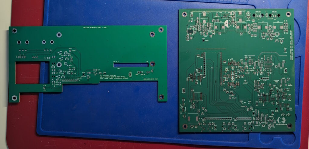
I placed an order for four different PCBs from JLCPCB:
- The main board, which would host the MCU / ADC, primary analog circuitry, and DC/DC converters. This was the most complicated component, with four layers and about 150x150mm surface on which to mount over 200 discrete parts.
- A front panel PCB hosting indicator LEDs, mechanical switches, pots, and mounting bosses for the OLED display
- A tiny breakout PCB for the USB-C power connector
- The front panel itself was fabricated as a single-sided aluminum PCB (with no copper layer)
When I unpacked them, I did have a small moment of panic. That is a lot of pads to solder correctly. I mostly use surface-mount parts these days; it is much more compact than through-hole, and especially on a board where the ground plane is critical, the fact that most parts don’t mean more holes to break up the plane should improve the signal quality.
I generally stick to 0805 and 1206 passives and SOIC or other 1.27mm-pitch ICs. Parts at that scale are easy to place. I use the hot air pencil method to solder. It works very well for passives and transistors. I often find some bridging on SOICs but it is straightforward to clean up with braid. Some of the parts for this PCBA were unavoidably only available in SOT-23-6. At 0.95mm pitch it’s not as bad as TSSOP, but I knew this still means the solder paste would leave a lot of bridges behind. And the small body size / low thermal mass makes them pretty fragile; you can only hit them with a soldering iron for so long before they pop.
Placing all the parts took an entire afternoon. Solder paste typically has an 8 hour working life on the board and I used almost all of it to make sure I didn’t make any errors or miss anything. (Slightly trickier than usual since I had also deliberately added some footprints for DNP parts in case I needed some workarounds for things I was less confident about.)
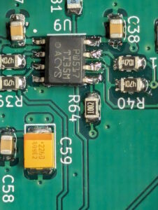
This worked out much better than it could have, though! I spotted a few pins that needed cleaning up across some of the ICs but I was able to clean all of it up. The SOT-23-5 Boost converter was the worst of it; there was some solder shorting two pins together that would not come off with some braid and a soldering iron; surface tension just kept it stuck in place. I was worried that I was giving it a bit too much punishment, and wound up desoldering the whole thing with the hot air gun. That action cleaned it up nicely and I was able to stick it back down again, and amazingly it still worked.
PCB Thoughts
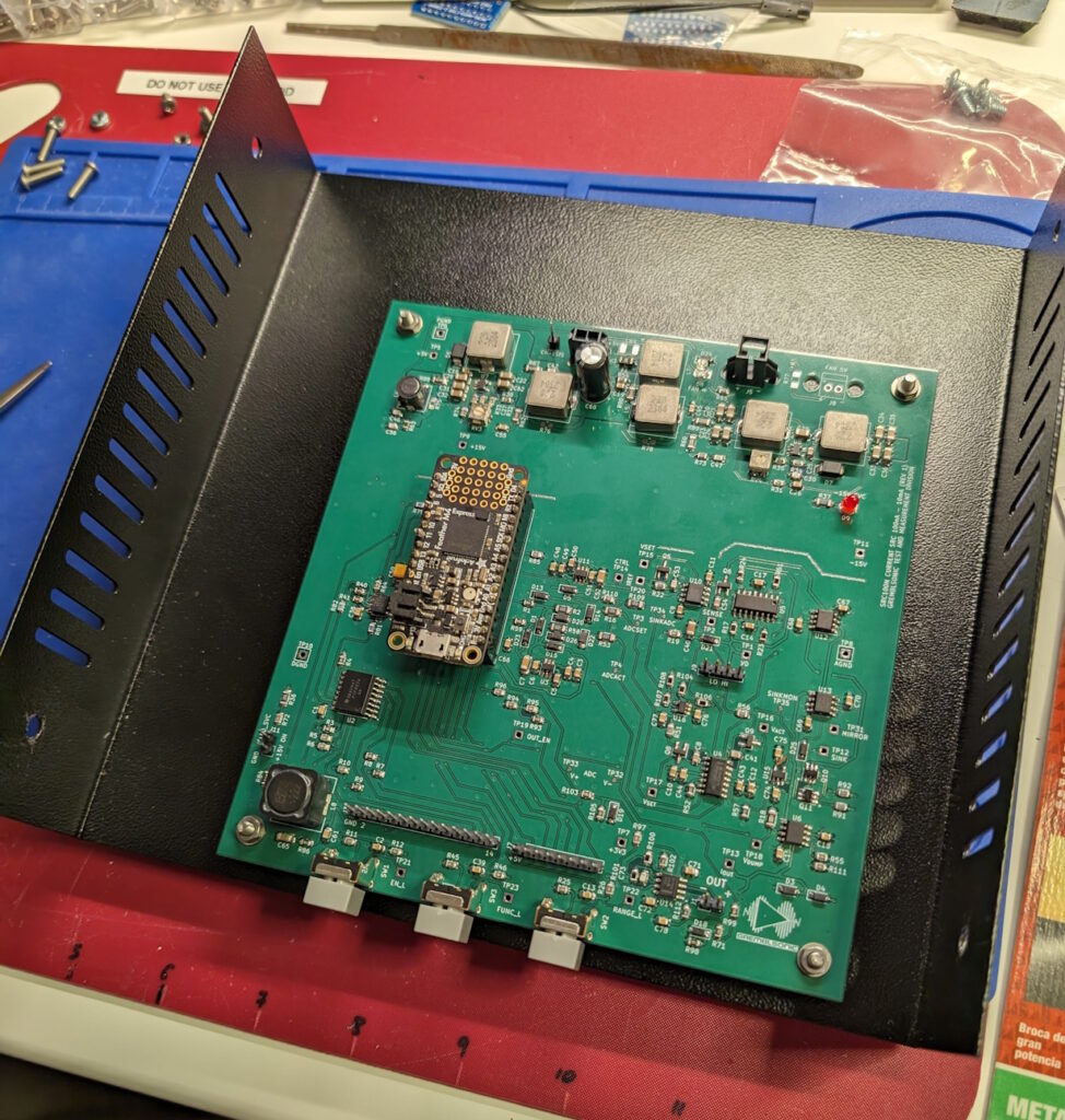
I mounted the three main buttons on the main PCB instead of the front panel PCB. This functions just fine and in the end was successfully assembled, but it meant I had to pretty carefully align the main PCB mounting holes with respect to the front panel. The tolerance was also fairly tight (0.5mm on each side of the buttons) which made for a nice, close fit, but also means that if the front panel were slightly misaligned, the buttons would jam. Good enough, but added complication that wasn’t needed. I should have just used a longer pin header on each PCB and sent the button signals and 3.3V power to the front panel (or used voltage dividers to work down the 5V signal to MCU-friendly 3.3V, like I did with the source/sink toggle switch).
Surprisingly, given how many parts and traces this involved, the boards did actually work great! The only board error I could find is some mislabeled test points. A minor nonfunctional issue like that, I can totally live with and be happy with the result.
I also found that there was not a lot of clearance between the micro-USB connector on the Arduino and the front panel PCB. This was a surprise given that the Arduino is basically centered on the board. It looks like there is plenty of room, but the strain relief on a USB cable makes it awkward to jam in there, which was necessary for updating the MCU firmware with a new image. (That, or pulling the MCU out of the instrument entirely.) A bit more clearance (1cm or so) would have been helpful. Cable bend radius can get big, quickly! But I also wanted to keep the digital domain as far away from the power supply domain as possible, and moving it up would have started to get closer than I wanted (or require a bigger board).
The aluminum PCB as the front panel itself had pros and cons. It was super cheap, and I did get 2 of the 5 aluminum panels that looked good. The overall yield was low, though, so I can imagine a scenario where the gamble didn’t pay off.
Further assembly
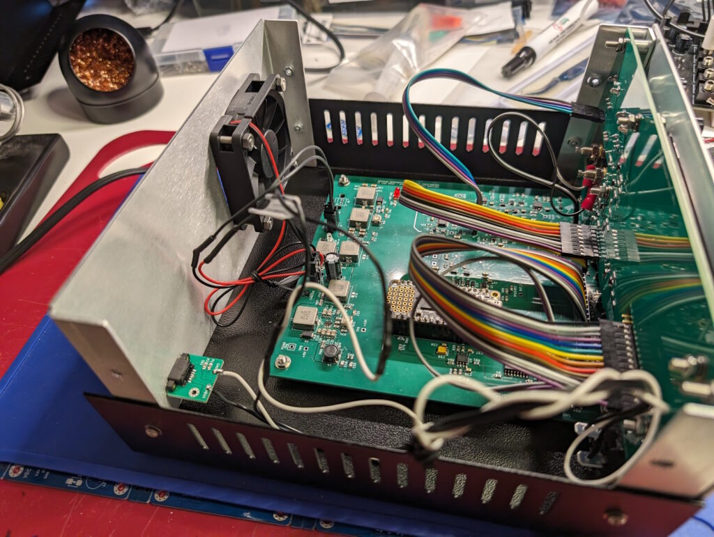
I also put all the parts on the front panel PCB at the same time. Then mounted the OLED display on that with some screws and standoffs, and connected everything together with some cable assemblies with simple Dupont connectors. The MCU was an Arduino Feather M4 Express, which is its own mini-PCB with holes for pin headers along the sides. I added the matching female sockets on the main PCB and pushed it into place.
The Hammond case was surprisingly hard to machine. Even thin steel is tricky to drill! I needed to put four holes in the base for mounting the main PCB, at fairly precise positions relative to the front panel, to align the buttons. It’s a lot slower going than cutting aluminum, and I had to start with small pilot holes and work my way up to holes big enough for the M3 screws.
When I turned it on, I was surprised (relieved!) that the power domains all worked correctly. It doesn’t draw too much through the USB socket for the USB supply (it will even run off a USB powered hub attached to a PC). The +15 and -15V regulators also operate smoothly, and were quickly dialed in with a pair of trimpots. The LC filtering on the 5V input keeps the ripple in the digital power domain low, and the analog voltage rails (with their own LC filters, snubbers, and decoupling capacitors) are whisper quiet at < 20 mVpp ripple each.
The MCU also turned on just fine, status LEDs light up, and the op-amps seemed to be doing their thing… but no display. My first assumption was that the LC filter I put ahead of the power feed to the display (to quiet down the noise generated back onto the main 5V supply rail by the OLED’s own 9V boost converter) was being troublesome–perhaps 2.2mH of inductance was pushing it. Probing the OLED power input with a scope showed it did have some fairly high ripple oscillation to it (about 1Vpp!), and while the average voltage was in spec, I wouldn’t have been surprised if the ripple was causing it to dip too low and maybe trigger a reset, or fail to operate the display’s boost converter.
I also probed the control signals that were being sent to the display from an I2C expander and… they were all silent. That’s not right. The connection is one-way, and the MCU should have been sending a steady stream of updated commands for what to display even if the screen were absent. So then I started checking connectivity for the I2C level shifter and bus expander. Then I noticed what looked like some unfused solder paste, and a bigger problem:
The pins of the I2C level shifter were not all aligned to the pads, it was a bit skewed to one side. Most of the pins had proper connectivity but the one in the lower right had about 1 Megaohm of resistance to the nearby resistor. Not quite an open circuit, but definitely malfunctioning. A few seconds of hot air made it snap right back into place, though. The next time I turned it on, the screen came up beautifully. If the ripple on the OLED power input was out of spec, it certainly wasn’t complaining.
The color gradient in the photo above is not actually visible to the naked eye. The OLED display has a PWM refresh rate of about 22 kHz, which interacts with the digital camera’s own sampling rate to create a slow blanking effect. In person, the screen is a uniform, sharp bright color with no visible flicker. Very different than playing around with it on a breadboard!
Calibration & results
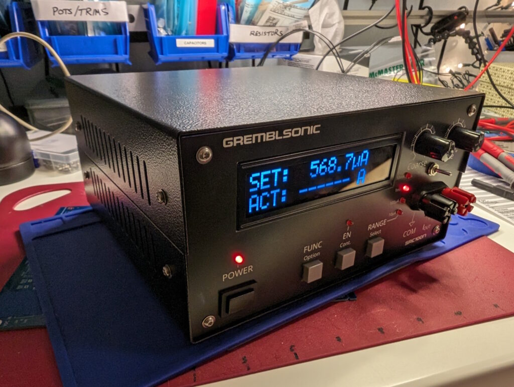
I had developed a calibration protocol in the Arduino MCU. The instrument would guide you through a set of currents to set with the front panel pots, and measure on an external ammeter. You would then enter the true current and lock it in; the MCU would sample the ADC for several captures and associate the ADC reading with the “true current” value entered by the user. This was repeated at several points along the calibration curve.
Entering data was a bit tricky with three buttons. I hit on a design where you could enter a six digit integer; one button changed the current digit from 1, to 2, 3, up to 9 and then back around to zero; another button moved the cursor one position to the right, and the last button locked it in. This was tedious when starting from zero but then I changed it to set the value based on what it should be and you just had to modify a couple of digits, which is much faster. To simplify things, you just entered an integer; it would ask you for a value in whole nanoamps or microamps depending on the range for the expected current.
It took a bit of time to get this to come together. A math error in the code caused everything to be off by about 10%. And the calibration process was initially a bit too clever, and required you to enter too many readings. I initially had a plan to explicitly calibrate the different gain ranges relative to one another. I realized I was adding more error than I was eliminating though. The gain range resistors were 0.1% tolerance and just hard-coding their resistances to the nominal values both simplified the process and gave greater accuracy.
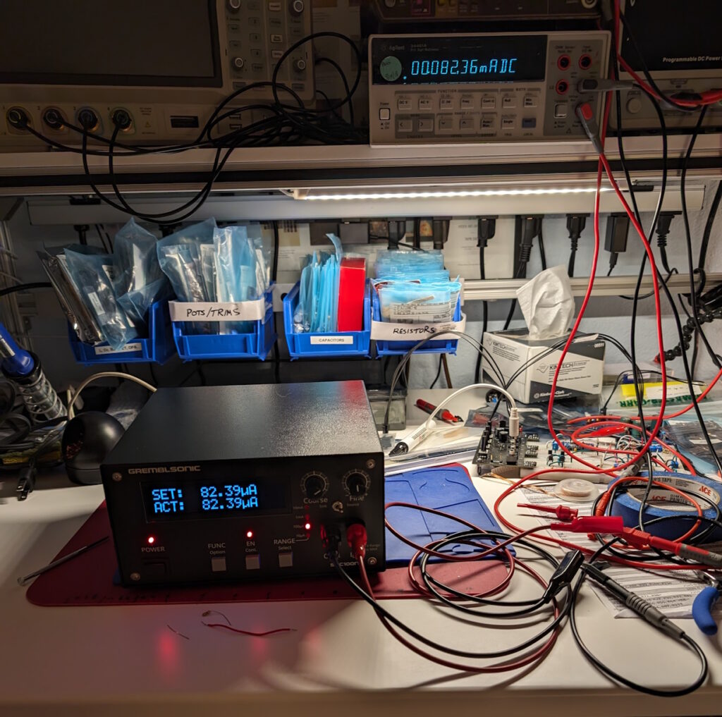
In the end, this performed incredibly well. Over the whole extent of the current it can drive, the current measurement capability is accurate to within 0.1% of the selected range! This isn’t true at the extreme low end; there’s a minimum resolution of about 50nA, and some oscillation in the tens of nA’s that makes it less than perfectly rock stable at the low end. But this is actually beyond the level of control I actually need. I’m really happy with this result!
The voltage sensor isn’t nearly as good as the current measurement. As described in part 1, I didn’t use separate amplification ranges to handle different input scales, as I didn’t want to pay for (or find room on the board for) the two extra SP4T analog switches it would require, along with more expensive precision resistors. It was very much a secondary feature, and it showed; the accuracy over the -15V to +15V range is only true to within about 20mV. I’m not quite sure why the accuracy is so poor; the offset voltage of the OPA192 is low enough that on paper this should be good to measure down to 1/2 mV precision. I might dig into this some time soon and see if I’m making a stupid mistake in the ADC or calibration code. In any case, this is good enough to get a general feel for the voltage of the connected device (or take resistance measurements to about 5% accuracy), but I won’t be ditching my DMM any time soon. It’s no Keithley SMU. Then again, at about 1/20 the cost, it’s no Keithley price tag either!
This was fun to build and definitely pushed my design skills a bit further. I’m really pleased I was able to assemble everything with no major mishaps, and I find it kind of incredible that you can put these kinds of components together and get this level of precision. The ADC on the SAMD51 MCU isn’t that impressive on paper (< 12 ENOB, and error up to 19 LSBs), but with an external reference, slow reads / oversampling, and a good calibration routine, you can measure small values with surprising precision and accuracy.
Related work
If you’re interested in homebrew SMU tech, Dave Erickson’s DIY-SMU project is a much more worthy attempt here. His is a true digitally-controlled SMU, with a graphical touchscreen, SCPI computer control, a vastly higher voltage range of ±150V and higher current range of 1µA — 100mA. Very cool! And a much more involved build.