
While working on a state-variable voltage controlled filter (VCF), I found that different waveforms (sine, saw, square) would come out attenuated to varying degrees. If the final amplifier stage is tuned to make the square wave reasonable and not clip, then sawtooth and especially triangle or sine waves were very quiet (7–7.5 Vpp out for 10 Vpp in, about 3 dB loss). Different resonance CV levels also caused the output signal to change amplitude significantly. Especially since I plan to cascade two, 12 dB / octave filter sections, this would result in too much attenuation for these signal shapes (6 dB total loss). This automatic gain control (AGC) circuit is designed to compensate for the -3 dB variable gain of each filter stage.
The surprising difficulty (rather, impossibility) of finding a low-distortion operational transconductance amplifier (OTA) driven AGC schematic I could use directly led to the development of the circuit presented here.
Target design requirements
This application expects a 7 Vpp input signal and amplifies it to a 10 Vpp low impedance output signal. It must maintain a 9.5–10.5 Vpp output for inputs between about 6 and 13 Vpp.
Specific design constraints on ICs are driven by the design of the the VCF stage intended to preceed this one, involving 3 OTAs (i.e. 1.5 IC’s) and 2 opamps, leaving 1 OTA free in a two-element OTA device. Without an AGC, the VCF would also require a third opamp as a fixed output gain / buffer stage, all implemented on a four-element TL074H (or two TL072H’s). These existing parts inform a design target for the AGC implementation of no more than one OTA and two general-purpose opamps.
Related work
AGC circuits are described in various places, but are either high-distortion, or difficult or impossible to implement as-is. The LM13700 OTA datasheet [1] shows an AGC circuit in Figure 25. This has the advantage of being a simple circuit with minimal additional parts. But the output stage will cause distortion by passing the OTA output current through a resistor potentiometer to ground for I-to-V conversion, with some fraction of that current then being passed through the Darlington buffers and into a large capacitor. Using an opamp for I-to-V conversion would give lower distortion. And more importantly, the reliance on the linearizing diodes for gain reduction means that the audio signal will not benefit from the linearizing diode effect when operating at the target gain level, adding further distortion.
Another common AGC architecture involves using a JFET as a voltage-controlled resistor to voltage-divide the input to an opamp configured as a noninverting amplifier [2]. JFET transistors, however, have notoriously poorly-controlled specifications with significant lot-to-lot variation. The ability to fully cut off the JFET when the signal is below target amplitude is also difficult to maintain as JFET’s often require significant negative VGS to enter cutoff.
The schematic that I found most helpful was from a Burr-Brown (now Texas Instruments) application note on uses of the OPA660 “diamond transistor” (OTA) [3]. Figure 19 shows the OTA (albeit represented by their diamond transistor symbol) used as a voltage-controlled amplifier (VCA), with the output buffered by an opamp, and a differential transistor pair amplifier used to reduce the control current to the OTA as the output (passed through a low-pass filter) exceeds a threshold voltage. This design would be cumbersome to implement as-is given the number of parts, cumbersome differential amplifier in place of an opamp, and reliance a JFET transistor. Moreover, both the OPA660 OTA and OPA621 opamp are obsolete components. But the diagram represents a useful starting point for design.
An overview of various AGC topologies (including the pointer to the Burr-Brown application note) is given in [4].
Circuit schematic
The circuit (shown in Figure 1) works in ngspice simulation as well as in testing on a breadboard. Square, sine, triangle, and sawtooth waves passed through a 12 dB / octave lowpass filter with a variable gain of between 0 and -3 dB all have normalized output of approximately 10 Vpp after correction by the AGC:
The circuit relies on a bipolar power supply of ±12V. To improve the PSRR of the circuit, any voltage levels that directly impact the output are referenced to ±8V signals generated by a combination of an LM4040 voltage reference Zener diode and an opamp (not shown) rather than Vcc+.
Theory of operation
The working principle of the circuit is based around using the OTA and one opamp as a voltage-controlled amplifier (VCA) and output buffer. A fixed 375μA control current and 200μA linearizing diode current, along with the 100 kOhm I-to-V resistor R11, set the nominal gain of the circuit.
The output is half-wave rectified and put through a 17 Hz low pass filter (2k resistor and 4.7μF capacitor). This produces a stable “rms value” from the output, which is compared to a threshold voltage controlled by a trimpot. Another opamp is configured as a current source, with differential inputs comparing Vrms and the threshold voltage. If Vrms is less than the threshold, the current source is off. When active, the output current increases as Vrms exceeds the threshold by greater amounts.
This current is fed, in turn, into a Wilson current mirror that “steals” current from the fixed 375μA control current, reducing the VCA gain and locking Vrms to the threshold voltage through negative feedback. As the Vrms – threshold difference increases, the theft current is eventually limited as the current source and mirror run out of voltage headroom, and does not completely eliminate the control current, so very large input signals will cause the output to rise above the 10 Vpp regulated output amplitude.
The cutoff frequency of the RMS accumulator is approximately 16-17 Hz. As such, the worst case response latency for the AGC to adjust to a change in input amplitude is around 50ms. The 100nF capacitor C7 helps accelerate the response attack, while adding a mild undershoot when first scaling down the output voltage.
Performance
The design objective of the application circuit is to provide a nominal gain of 3 dB to raise a 7 Vpp reference signal amplitude input to 10 Vpp output. It should constrain the amplitude of its output to approximately 10 Vpp over at least a range from 7-14 Vpp input amplitudes.
Simulation
A simulation was prepared with ngspice to test the circuit design. The potentiometers RV1 and RV2 have been adjusted within the simulation to provide tuned values to center the output and scale the gain response appropriately.
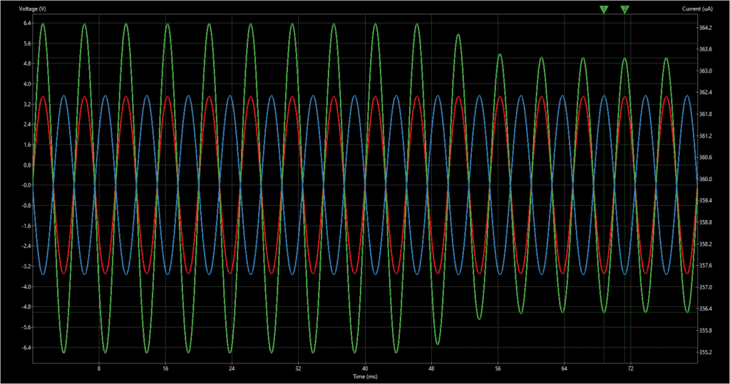
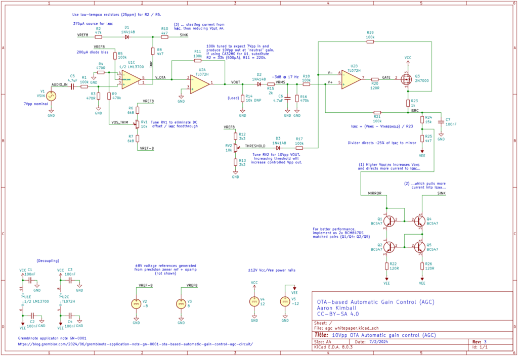
Figure 2 shows the circuit providing the intended 3 dB gain when operating in scale-up mode. The reference signal (red) is a 7 Vpp sine wave at 200 Hz. This is preamplified by -1x to send a 7 Vpp input signal (blue) to the circuit under test. After 50 ms, the AGC adjusts to produce a 10 Vpp output signal (green).
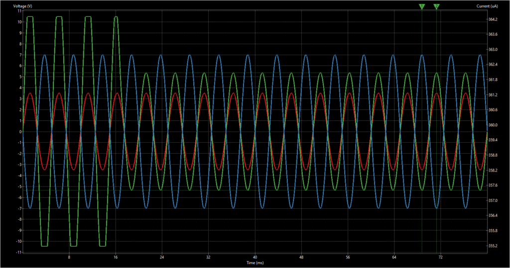
Figure 3 shows the circuit automatically reducing its gain to < 0 dB when presented with an oversize input signal. The reference signal (red) remains a 7 Vpp sine wave at 200 Hz, but this time preamplified by -2x to drive a 14 Vpp input signal (blue) into the circuit under test. The output is initially clipped but quickly charges the VRMS capacitor, and after 16 ms, the AGC adjusts to produce a 10.7 Vpp output signal (green).
The input signal gain of +6 dB between the first and second cases produces a relative output signal gain of just 0.6 dB, showing the successful implementation of the design concept.
Bench testing
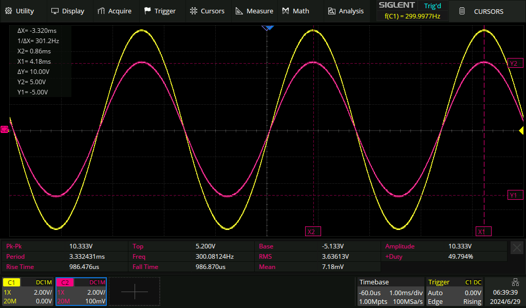
Empirical testing of the same circuit on a breadboard showed even better results, with a 7 Vpp input sine wave at 300 Hz produced by a Siglent SDG1025 function generator yielding a 10 Vpp output (measured on a Siglent 2104X+ oscilloscope) after circuit calibration (Figure 4). The output amplitude ranged from 9.8 to 10.3 Vpp with input signals ranging between 5.2 and 15 Vpp (Figure 5). The 15 Vpp input has a gain of 6.6 dB relative to the 7 Vpp reference input, and the 10.3 Vpp output has a gain of just 0.26 dB relative to the 10.0 Vpp reference output.
When using the prototype VCF stage as input, audio rate sine, sawtooth, triangle, and square waveforms all produced output amplitudes between 9-10 Vpp. When significant resonance feedback was added to the VCF response, the high frequency resonant overshoot and undershoot peaks did not materially impact the RMS voltage of the VCF output signal and thus did not overly clamp the AGC audio output amplitude. The combination of high resonance and a low VCF control voltage so that the resonance dominated the VCF output would ordinarily result in a large signal that may be clipped by a fixed-gain output buffer opamp, but this signal was also appropriately clamped to 10.5 Vpp by the AGC (excluding the resonant overshoot excursions).
Bill of materials
| Ref Designator | Part description or MPN | Alternate part / MPN | Qty |
|---|---|---|---|
| C1-C4, C7 | 100 nF X7R 10% MLCC | 5 | |
| C5, C6 | 4.7 uF X7R 10% MLCC | 2 | |
| D1-D3 | 1N4148 | MMSD4148T3G | 3 |
| Q1, Q2, Q4, Q5 | BC547 | BCM847DS (x2) | 4 |
| Q3 | 2N7000 | 2N7002 | 1 |
| R1, R17-R19, R21 | 100 kOhm 1% resistor | 5 | |
| R11 | 100 kOhm 1% resistor | 220 kOhm 1% 25ppm | 1 |
| R5 | 100 kOhm 1% resistor | 100 kOhm 0.1% 25ppm | 1 |
| R2 | 47 kOhm 1% resistor | 33 kOhm 0.1% 25ppm | 1 |
| R3, R4 | 470 Ohm 1% resistor | 2 | |
| R6, R7 | 6.8 kOhm 1% resistor | 2 | |
| R8, R10, R25 | 4.7 kOhm 1% resistor | 3 | |
| R12, R13 | 3.3 kOhm 1% resistor | 2 | |
| R9, R16 | 470 kOhm 1% resistor | 2 | |
| R14 | DNP | ||
| R15 | 2 kOhm 1% resistor | 1 | |
| R20, R22, R26 | 120 Ohm 1% resistor | 3 | |
| RV1, RV2 | 10 kOhm trimpot | Bourns 3362P-1-103LF | 1 |
| U1 | Texas Instruments LM13700DR | Alfa AS3280D* | 1 |
| U2 | Texas Instruments TL072IDR | Texas Instruments TL072HIDR** | 1 |
* AS3280D is the Alfa reproduction of the CA3280 OTA, an upgrade pick over the LM13700. Note that this is not pin-for-pin compatible.
** TL072H has lower Vos and better all-around specs than the original TL072. Its output common mode range is wider, which will also allow the AGC to maintain compliance over a wider range of input signal amplitudes than the TL072. This is pin-for-pin compatible in an identical IC package and approximately the same price.
Integration and modification notes
R14 is shown as a 10k resistor, but this should be substituted for your output/load and does not need to be directly placed.
The AGC is calibrated by two trimpots; one to set the overall circuit gain and another to zero out any Vos or Iabc feedthrough offset. Zeroing the offset allows the most accurate reproduction of the input signal over the widest amplitude compliance range. To calibrate, feed a sine wave at the nominal input voltage (7Vpp) to the input and trim RV2 so the top of the output waveform is at +5.00V, then trim RV1 so the bottom of the output waveform is at -5.00V.
If using an LM13700, the output buffer is unused. If using AS3280 / CA3280 instead, two resistors (R2 and R11) should be changed due to the OTA gm of 16 instead of 19.2 * Iabc (see alternate parts column in the BOM). R5 can also be upgraded to a 25ppm low-tempco resistor for better gain tracking across the operating temperature range.
For applications targeting a different output amplitude, you can adjust the nominal amplification factor over a range of about 2x by tuning the threshold voltage and offset via the potentiometers RV1 and RV2. While the precise value of R11 is not critical due to the wide adjustment range of the potentiometers, scaling the value of R11 up or down based on your desired nominal gain factor will help the AGC maintain compliance over a wider working input amplitude range centered around your nominal input signal Vpp.
The LM13700 and the AS3280 each include two OTA elements, however this circuit consumes only one of them, leaving the other available for use as a VCF, VCA, or other subcircuit. The unused element is not shown on the schematic.
Higher PSRR is achieved by using a local 8.00V reference generated from an LM4040 and an opamp (not pictured in the schematic) rather than connecting the Iabc / Id input current set resistors directly to the Vcc+ rail. The simple resistor scheme for setting Iabc does have temperature coefficient-driven variation. Temperature variation can be at least partially mitigated by choosing low-tempco resistors, although that will not help cancel the VBE tempco inside the OTA. Using a current source in place of each of R2 and R5 (or just R2 if you are using an AS3280 [5] / CA3280 instead of the LM13700 shown) would offer more stable performance and eliminate the VBE temperature dependence, at the cost of an additional opamp and transistor.
The control current and diode bias current are set by resistors R2 and R5. The input diodes of the OTA sit at 2x VBE above Vcc (about -10.8V as-shown), so the currents can be calculated as (8.0 – (-10.8)) / R. This circuit can be adapted for a wider power supply range like ±15V by adjusting the resistor values to provide the same current over the 3V wider differential between a -15V Vcc- and the 8V reference voltage, or by using a current source to control these inputs. As shown, the circuit response will vary with large fluctuations in Vcc-, although the 100nF decoupling capacitor on the LM13700 provides the necessary PSRR for most cases.
The circuit is shown with a four transistor Wilson current mirror. Precise current mirroring is not critical as the appropriate theft current will be driven by negative feedback. Cost or space conscious applications could employ a three or two-transistor current mirror implementation with a potential tradeoff of loss of compliance headroom in input amplitude range. By contrast, a more precise current mirror can be delivered in a compact footprint with two SOT-23-6 BCM847DS matched transistor pairs implementing the four transistor mirror, which will maximize compliance headroom.
References
- LM13700 Dual Operational Transconductance Amplifiers With Linearizing Diodes and Buffers (datasheet). Texas Instruments, 2015. Retrieved from Texas Instruments’ website: https://www.ti.com/lit/ds/symlink/lm13700.pdf
- Bhatt, Ashutosh. Circuit Design: Automatic Gain Control. Retrieved from Engineer’s Garage: https://www.engineersgarage.com/circuit-design-automatic-gain-control/
- Henn, Christian. Automatic Gain Control (AGC) Using the Diamond Transistor OPA660 (Application Note No. sboa072). Retrieved from Texas Instruments’ website: https://www.ti.com/lit/an/sboa072/sboa072.pdf
- Martinez G., Isaac. Automatic Gain Control (AGC) circuits: Theory and design. University of Toronto, 2001. Retrieved from citeseer: https://citeseerx.ist.psu.edu/document?repid=rep1&type=pdf&doi=b438ae7f03f92d0cfbe37f0919667f4b907c2224
- AS3280 – Dual Operational Transconductance Amplifier (OTA) (datasheet). Alfa Rpar, 2019. Retrieved from Alfa Rpar’s website: https://www.alfarzpp.lv/eng/sc/AS3280.pdf
Revision notes
Rev. 2 (6/29/2024): Connected RV1 bias network to the inverting input of the OTA rather than opamp U2A and modified resistor values R6 and R7.
Rev. 3 (7/2/2024): Changed RV2 to 10k and R12/R13 to 3k3 for wider adjustment range; corrected gain resistor values R2, R5, and R11 for CA3280 case.